
Staff
Tetsuo Sasaki Professor / Hamamatsu

Research Area
Nonlinear optics, Terahertz spectroscopy, Crystal growth, Analytical chemistry
Research Detail
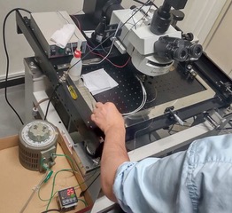
Development of THz laser spectrometer and its application.

Toru Aoki Professor / Hamamatsu

Research Area
Imaging technology of X-ray, gamma-ray and nutoron.
Research Detail
We research and develop the imaging devices, sysytems and its application for invisible light especially X-ray, gannma-ray and nutron from the base to practical use.

Hiroya Ikeda Professor / Hamamatsu

Research Area
Semiconductor engineering, Semiconductor device engineering, Semiconductor quantum physics
Research Detail
We are investigating new-functional and high-efficient devices using Si nanostructures and recently focusing on thermoelectric devices.

Wataru Inami Professor / Hamamatsu

Research Area
Optical Measurement Science,Advanced Microscopy
Research Detail
Developing principles for new measurement and imaging technologies which show us things we have not seen before.

Yoku Inoue Professor / Hamamatsu

Research Area
Semiconductor engineering, Crystal growth, Nanomaterial engineering
Research Detail
We are working on broad CNT researches including growth, fabrication of CNT constructions (fibers), CNT composites and CNT electronics.

Yoshinobu Ebisawa Professor / Hamamatsu

Research Area
Visual Information Engineering
Research Detail
Developments of video-based pupil detection technique and of pupil detection-based methodology and implementation (e.g., eye-gaze and head pose detection, and drowsiness detection) for human interaction and monitoring are done for the improvement of welfare medical treatment and safe driving.

Atsushi Ono Professor / Hamamatsu

Research Area
Near-field Optics, Plasmonics
Research Detail
We design and fabricate metallic nanostructures for the efficient surface plasmon exicitation. It is applied for the development of super-resolution imaging device and high-sensitive photodetectors.

Keiichiro Kagawa Professor / Hamamatsu

Research Area
CMOS image sensors, information photonics
Research Detail
Biomedical CMOS image sensors and computational imaging based on multi-aperture optics and advanced CMOS image sensors for ultra-fast or ultra-high-sensitivity imaging.

Yoshimasa Kawata Professor / Hamamatsu
川田善正.png)
Research Area
Laser microscopy,three-dimesinsional imaging theory
Research Detail
We have developed high resolution optical microscopy
and its applications to optical data storage. Nano-fabrication
techniques has been developed with femto-second laser
pluse.
Yukinori Ono Professor / Hamamatsu

Research Area
Semiconductor nanodevices
Research Detail
We are developping the technologies for manipulating single charges, spins, and phonons in silicon.

Shoji Kawahito Professor / Hamamatsu

Research Area
Imaging Semiconductor Devices and Systems
Research Detail
We are investigating imaging semiconductor (CMOS) devices with advanced performance and functions for scientific, industrial and biomedical applications.

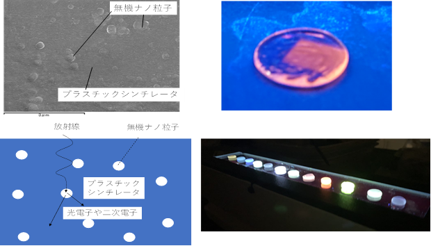
Masanori Koshimizu Professor / Hamamatsu
Research Area
Radiation Detection, Materials Science
Research Detail
Development of organic, inorganic, and organic-inorganic hybrid materials for radiation detection (scintillators and storage phosphors)
Takayuki Nakano Professor / Hamamatsu

Research Area
Semiconductor epitaxial growth, Group-III nitride
Research Detail
Development of novel functional devices using group-III nitride semiconductor epitaxial growth

Yoichiro Neo Professor / Hamamatsu

Research Area
Vacuum nanoelectronics
Research Detail
Cathode and physics: Field emission cathode, photocathode, etc. Apprication: High frequency Vacuum tube, image tube etc.

Gen Hashiguchi Professor / Hamamatsu

Research Area
Micromachining,Sensor
Research Detail
We have focused on MEMS design theory and its appliation for development of integrated MEMS with semiconductor devices.

Kazuhiko Hara Professor / Hamamatsu

Research Area
Semiconductor engineering, Solid-state physics
Research Detail
We have been developing unique light-emitting materials based on the semiconductor nanotechnology aiming at their application for novel light sources and displays.

Masato Futagawa Professor / Hamamatsu

Research Area
Semiconductor, Integrated circuit, Sensor
Research Detail
We are studying water content, ion concentration, pH, and temperature sensor devices using measurement technology, semiconductor process, and integrated circuit technologies. We developed environmental monitoring sensors integrated with their physical and chemical sensor devices.

Vygantas Mizeikis Professor / Hamamatsu

Research Area
Applied optics, laser fabrication,micro-/nano-photonics
Research Detail
Laser fabrication and characterzation of photonic micro-/nano-structures, modification of materials by femtosecond laser pulses.

Daniel Moraru Professor / Hamamatsu

Research Area
nanostructures, nanoelectronics, atomic devices
Research Detail
tunneling transport via dopant atoms in nano-transistors and nano-diodes; semiconductor device fabrication.

Akihisa Ogino Associate Professor / Hamamatsu

Research Area
Plasma Science, Plasma Application
Research Detail
We have been researching plasma processing that aims at modifying the physical and chemical properties of a surface and also fabricating nanomaterials.

Tetsuya Kouno Associate Professor / Hamamatsu

Research Area
Nano-micro photonics and structures
Research Detail
Optical properties based on nano-micro structures.

Hiroko Kominami Associate Professor / Hamamatsu

Research Area
Optical materials, Optical properties
Research Detail
Development of inorganic emitting materials for sterilization, long-afterglow, photodynamic therapy

Hiroaki Satoh Associate Professor / Hamamatsu
Research Area
Photonic devices
Research Detail
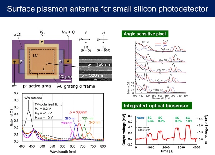
We are developing new silicon photodetectors with surface plasmon antenna to achieve high sensitivity and high functionality.
Masanori Takeda Associate Professor / Hamamatsu

Research Area
Terahertz technology, submillimeter-wave circuit, superconducting electronics
Research Detail
Toward terahertz (THz) applications, we have been studying on system stabilization of THz time-domain spectrometer and THz imaging technology.

Tripathi Saroj Raman Associate Professor / Hamamatsu

Research Area
Terahertz wave engineering
Research Detail
Terahertz spectroscopy, sensing and imaging.

Masahiro Hori Associate Professor / Hamamatsu

Research Area
Semiconductor engineering, Quantum electronics
Research Detail
We are developing a novel technique towards the manipulation of electronic charges and spins based on a quantum level in a silicon transistor.

Keita Yasutomi Associate Professor / Hamamatsu
Research Area
Research Detail

⬆️ Back to top